|
|
|
 |
|
|
|

MS1010
|
|
 |
|
|
|
 |
|
 |
|
|
|
|
|
 |
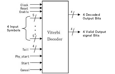
The MS1010 is an Area Efficient Viterbi Decoder IP core optimized for UWB (Ultra Wide Band) of ASIC hardware. The decoder is a Register Exchange, High performance and Low latency type of UWB Viterbi Decoder.
The circuit area of the decoder is Ultra Small realized by Mathematec's original LSI circuit design technology, SPINOR. Also, the performance has been verified by the actual LSI chip.
Additionally, we take the design change request on the IP core to meet the specification of our customer's product. |
|
|
 |
|
|
|
|
|
 |
– Constraint Length K=7
– Code Rate R=1/3 (Supports any Punctured Symbol with Soft-Value “0” input from outside)
– Generator Polynomials g0=[133]8, g1=[165]8, g2=[171]8
– Soft Decision Bit Depth 5
– Supports Tail Bit
– Optimized design allowing 480 Mbps operation
– Decoding Throughput 4 bits/clock
– Coding Gain in average (BER 10-5)
>> Approximately 5.5dB (equivalent to 60 Survival Path length while decoding PLCP Header)
>> Approximately 3.8dB (equivalent to 112 Survival Path length while decoding Payload)
– Latency (means total clock cycles from first signal input to first signal output)
>> 21 clocks (while decoding PLCP Header)
>> 34 clocks (while decoding Payload)
– Supports Cancel Decoding function (Decoding is canceled by cancel signal)
– Deliverables
>> Synthesizable Verilog RTL source code (Logic Synthesis is confirmed as shown in Figure 3)
>> Comprehensive Verification test bench and its vectors |
|
|
 |
|
|
|
|
|
 |
The Target Convolutional Encoder is shown in Figure 1.
K=7, R=1/3, g0=[133]8, g1=[165]8, g2=[171]8

Figure 1 Convolutional Encoder |
|
|
 |
|
|
|
|
|
 |
 Figure 2 Block Diagram
|
|
|
 |
|
|
|
|
|
 |
The size of this IP core is depended on a Delay Constraint shown as Figure 3, and our customer can choose any one of them.
Tools
Synopsys's Design Compiler
Version A-2007.12-SP2
Library ARTISAN TSMC 90nm Gen.
Logic Synthesis Constraints
1. Delay Constraints See Figure 3
2. Maximum Fanout Constraints non
3. Zero Wireload
4. Operating Condition Slow
|
|
Figure 3 Gate Counts & Delay
|
|
Note) Figure 3 shows the 2-input-NAND-equivalent gate counts.
|
|
|
 |
 |
|
|
|
 |
|
 |
|
|