|
|
|
 |
|
|
|
 |
|
|
|
|
|
 |
|
|
|
|
|
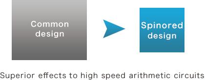
Have you ever dreamt of your LSI or FPGA with a saving power, lower cost or higher speed?
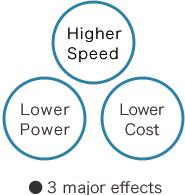
Do not you think it would be great if you could have your LSI enhanced to “Less Power Consumption”, “Smaller Size”, “Lower Latency” and “Lower Delay”? We mean these functional enhancements all together.
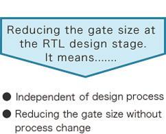
Although these enhancements might not be achieved by any other known technology, our innovative technology called SPINOR can achieve them on your circuits. Spinor is our unique RTL design technology for logical circuits and is independent of any LSI design process.
|
|
|
|
|
|
|
|
|
|
|
|
|
|
|
>>Moore's Law
It has been said that the Moore's Law related to LSI nanotechnology will last for the time being in spite of many engineering problems. However, the improvement rate of the power consumption and delay per a process reduction have slowed down.
For the next generation's process development, it will be more difficult to reduce the cost per a gate due to the necessity of a huge investment and uneasy technical problems they have to overcome. For those reasons, some IDMs (Integrated Device Manufacturers) have left from the next generation's process development.
>>The trend of System LSI development
Today, many more functional demands are expected on a single LSI chip, and we are on the verge of ostensible replacements of SOC (System on Chip) by SiP (System in Package). Therefore, a circuit size is getting bigger as well as the manufacturing cost. “Higher Speed”, “Lower Power” and “Lower Cost” are the requirements from the market, and LSI vendors have to try to meet them. For LSI vendors, it is, however, getting more difficult to keep competing on the market by meeting these demands, so that a smaller number of vendors shall lead the market; the vendors who provide superior IP cores to others.
|
|
|
|
|
|
|
|
|
|
|
|
|
|
|
Being our most important confidential technology, we cannot reveal detail information about Spinor. Yet, let us outline Spinor design procedure.
|
|
 |
|
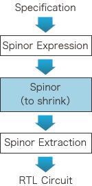
Spinor is the technology to design electric circuits with mathematical procedures which is different from Logic Synthesis or Behavioral Synthesis. Spinor design procedure is as follows.
First of all, the digital circuit specification is mapped to some mathematical expression, called Spinor expression. The expression is thereafter transformed (Spinored) to the shrinkable format. At this stage, redundant parts of the circuit are easily taken away, and the only essential parts are extracted; we call this procedure the Spinor extraction. The result is optimized therefore a smaller circuit, which still meets the same specification. |
|
|
|
|
|
|
|
|
|
|
|
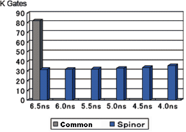
The following figure shows the example that the delay is reduced by Spinor design. As you can see, the gate count is drastically reduced also.
|
|
 |
|
|
In this case, our customer initially designed some circuit by a common RTL design technique. However, they could not reduce the delay constraint no less than 6.0ns by logical synthesis. Also, they could not reduce the gate count less than 80 K gates even if the delay constraint is 6.5ns. On the other hand, our Spinor design has achieved the delay constraint of 4.0ns with reducing gate count by more than a half.
The Spinor design was used, in this case, to reduce the delay based on the customer's request.
As this example, Spinor can realize less delay and less gate count simultaneously by removing the redundancy of the logical circuit designed by common techniques.
Note) The above numeric value is one of many examples. It is not guaranteed that every Spinored circuit will have the same effect. |
|
|
|
|
|
|
|
|
|
|
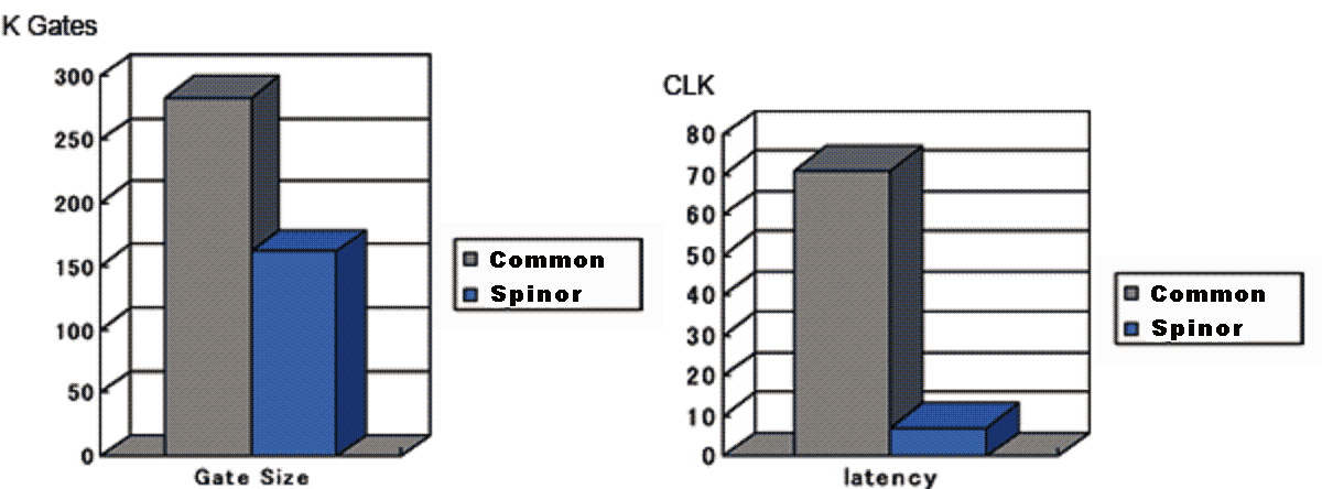
The following figure shows the example that the gate count is reduced by Spinor design. As you can see, the latency is drastically reduced also.
|
|
 |
|
Note) For the latency value, the theoretical limit (128 clocks) is removed.
Comparing with the common RTL design technology, Spinor reduced the gate count by more than 40%.
The Spinor design was used, in this case, to reduce the latency drastically based on the customer's request. If the Spinor design were used with a little bigger latency constraint, the gate count would be smaller.
As this example, Spinor can realize smaller gate count and shorter latency simultaneously by removing the redundancy of the logical circuit designed by common techniques.
Note) The above numeric value is one of many examples. It is not guaranteed that every Spinored circuit will have the same effect.
|
|
|
|
|
|
|
|
|
|
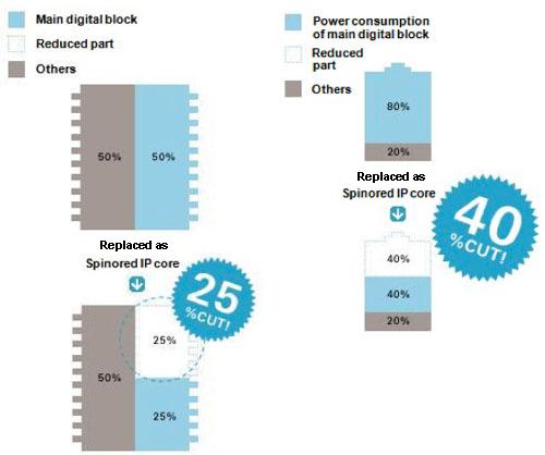
| The following figure shows the example that the power consumption is reduced by Spinor design. As you can see, the circuit area is reduced also. |
|
|
|
Comparing with the common RTL design technology, Spinor reduced the power consumption by 40%.
The Spinor design was used, in this case, to reduce the power consumption of the arithmetic circuit based on the customer's request. If the Spinor design were also used for other 50% of the circuit, it would be possible to reduce both of the power consumption and gate count much more.
As this example, Spinor can realize saving more power consumption and less gate count simultaneously by removing the redundancy of the logical circuit designed by common techniques.
Note) The above numeric value is one of many examples. It is not guaranteed that every Spinored circuit will have the same effect
. |
|
|
|
|
|
|
|
|
|
|
|